
Have you ever been hit with that ultimate question from your boss or a client: “Can we make this millimeter-wave (mmWave) phased array antenna any cheaper?”
Let’s be honest. Every time I look at the Bill of Materials and see the pricing for T/R (Transmit/Receive) modules, I have to take three deep breaths. For a standard 64-element array, the T/R modules alone swallow up most of the budget, and when you toss in high-frequency PCB materials, anechoic chamber testing, and precision manufacturing—your costs instantly redline.
In this article, I’ll share my firsthand experience and the lessons learned from years of navigating cost reduction in phased array development. Hopefully, these insights will save your next project’s budget.
1.Why Is Phased Array Hardware So Expensive? Break Down the Cost Structure
Every RF engineer who has managed a phased array project knows it is a capital-intensive endeavor. However, to cut costs effectively, you must first understand exactly where the money goes. Let’s break down the typical cost distribution to give you a clear benchmark.
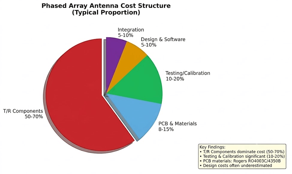
If we look at the cost of a phased array antenna as a pie chart, T/R components consistently consume 50% to 70% of the total budget. These modules house power amplifiers (PAs), low-noise amplifiers (LNAs), phase shifters, and attenuators. Every single channel adds up quickly.
1.1 T/R Modules — The Ultimate Cost Killer
In the mmWave spectrum, T/R module pricing varies drastically based on the application:
Consumer Grade (77GHz Automotive Radar): Can be sourced for tens of dollars.
Space-Qualified / Military Grade: High-performance channels can run anywhere from hundreds to thousands of dollars per single channel.
Aerospace-Grade Gallium Nitride (GaN) Modules: These can easily cost thousands to tens of thousands of dollars per set. A single missile-borne radar requires hundreds or thousands of these modules, pushing total costs into millions of dollars.
An Counter-Intuitive Fact About Scalability: As the number of antenna elements increases, the total cost does not scale linearly. For instance, a 64-element array might cost between $15,000 and $75,000 (approx. 100k–500k RMB), while a 256-element array might cost $75,000 to $300,000 (approx. 500k–2M RMB). While the element count quadruples, the cost only increases by a fraction. This is because infrastructure components—like the beamforming feed network and power supply units—can be shared and multiplexed.
Pro-Tip from the Field: When calculating your initial project budget, never use a simplistic “element count × unit price” formula. Always factor in the shared cost distribution of the beam-control circuitry, feed networks, and power modules. Quotations provided by component vendors often omit these shared system-level integration costs.
1.2 High-Frequency PCB Materials — The Hidden Expense
While everyone focuses on the silicon and chipsets, the substrate material remains a major hidden cost. Millimeter-wave frequencies are unforgiving; standard FR-4 substrates fail due to high insertion losses and poor impedance stability. Engineers must rely on premium high-frequency laminates like Rogers RO4003C or RO4350B.
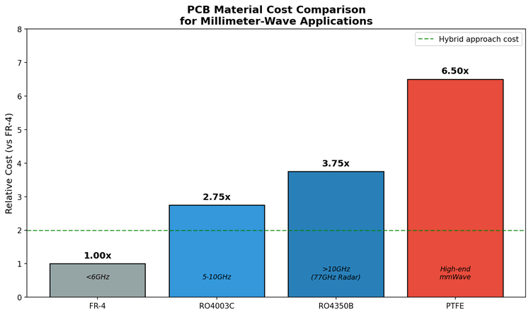
The cost differential isn’t just about the raw material; it’s heavily tied to manufacturing yield. High-frequency boards demand strict impedance control (often within ±5%) and tight line-width tolerances. Consequently, the yield rate drops significantly compared to standard multi-layer digital boards. A 16-layer high-frequency PCB can easily cost over three times more than a standard 4-layer board, driving up fabrication costs by 15% to 30%.
1.3 Over-the-Air (OTA) Testing & Calibration — Time Is Money
Phased array testing and calibration costs are routinely underestimated. I’ve reviewed multiple projects where the hardware BOM looked excellent on paper, but the final testing fees completely broke the project budget.
The expenses stem primarily from two bottlenecks:
Anechoic Chamber Rental: Full-band testing for a 64-element array typically requires 8 to 12 hours. A 256-element array can take 2 to 3 days. Renting a compact antenna test range (CATR) costs roughly $75/hour (500 RMB/hour), while large-scale 10-meter chambers can run up to $300/hour (2,000 RMB/hour).
Array Calibration: High-precision arrays require channel-by-channel phase and amplitude calibration. Manual or semi-automated tuning can cost $7 to $15 (50–100 RMB) per channel. For a 1024-element array, calibration alone can exceed $15,000 unless you invest heavily in proprietary automated calibration fixtures.
1.4 Engineering Design Costs — Software and Multiphysics Simulation
Don’t overlook front-end R&D expenses. Annual licensing fees for industry-standard electromagnetic simulation software (such as ANSYS HFSS or CST Studio Suite) range from $7,000 to $30,000 (50k–200k RMB) per seat.
Furthermore, simulating large-scale arrays (>1000 elements) demands high-performance computing (HPC) clusters, with single simulation runs taking hours or days. When you factor in thermal-mechanical-electrical multiphysics co-simulation to prevent thermal throttling, design overhead increases by another 20% to 30%.
Additionally, developing beamforming algorithms for FPGA/DSP hardware (like the AMD/Xilinx Zynq UltraScale+ architecture) requires specialized engineering talent, often incurring $30,000 to $75,000 (200k–500k RMB) in development costs.
2.Seven Proven Cost-Reduction Strategies for RF Engineers
Here are seven practical engineering strategies I have personally implemented that yield the most significant cost savings.
2.1 Strategy 1: Chip Localization and Components Substitution
This is the most immediate way to slash your BOM. Geopolitical supply chain shifts and trade restrictions have accelerated the adoption of alternative semiconductor foundries and localized T/R chip designers.
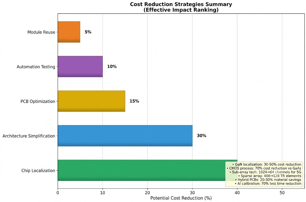
Upgrading to alternative localized Gallium Nitride (GaN) chip options can reduce component costs by 30% to 50%. A high-performance T/R chip that previously commanded premium import pricing can often be replaced at half the cost.
Trend to Watch: CMOS architecture is steadily displacing traditional GaAs (Gallium Arsenide) and SiGe (Silicon Germanium) processes in mainstream applications. For 77GHz automotive radars, CMOS-based MMICs reduce chip costs to roughly 30% of early GaAs alternatives.
Case Study: A specific satellite phased array project utilized sparse array technology to reduce the required T/R elements from 400 down to 128. By optimizing the array thinning architecture, the team bypassed massive component procurement costs while maintaining acceptable radiation patterns.
2.2 Strategy 2: PCB Substrate Optimization — Hybrid Layer Stacking
Material selection should match your exact operational frequency; over-engineering is a needless expense. Here is a quick guideline for substrate selection:
Below 5 GHz: Standard FR-4 is perfectly adequate. Do not waste budget on high-frequency laminates.
5 GHz to 10 GHz: Rogers RO4003C offers the best balance of low dissipation loss and moderate pricing.
Above 10 GHz: Standardize on RO4350B or advanced PTFE-based materials.
The “Hybrid Stack-up” Technique: Instead of making the entire multi-layer board out of expensive Rogers materials, use a hybrid fabrication process. Use RF laminates only for the critical top high-frequency routing layers, and use standard FR-4 for the internal low-frequency control and power routing layers. This approach is widely adopted in 5G macro gNodeBs and radar control boards, dropping PCB fabrication costs by 20% to 30%.
2.3 Strategy 3: Balancing Array Size and Performance (Design for “Good Enough”)
Over-specifying performance targets is a frequent pitfall. Designers often chase maximum gain, narrowest beamwidths, and ultra-wide scanning angles, causing costs to spiral out of control
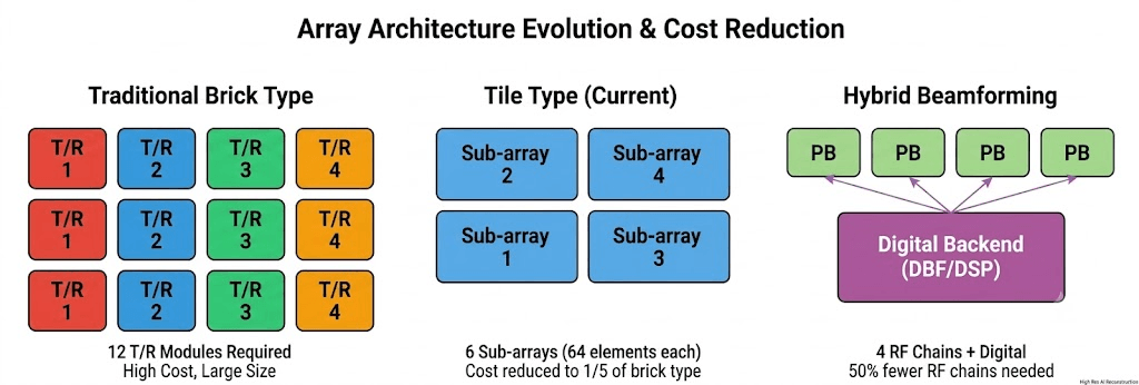
Often, system requirements can be met with smarter architectures. For example, in 5G small cell deployment, replacing a full 1024-element array with a 64-element sub-array module architecture is highly effective. Sub-array configurations reduce the absolute number of front-end RF chains while leveraging digital backend algorithms to compensate for performance trade-offs.
2.4 Strategy 4: Hybrid Beamforming (HBF) — The Digital/Analog Balance
While Digital Beamforming (DBF) offers maximum flexibility and performance, it is cost-prohibitive because every single Transmit/Receive unit requires a dedicated ADC/DAC channel.
Hybrid Beamforming (HBF) serves as the ideal compromise. It handles coarse beam steering in the analog domain (via analog phase shifters) and fine-tuning in the digital domain. This hybrid architecture slashes the number of required high-speed RF transceivers and data converters by over 50%, immediately lowering hardware complexity and cost.
2.5 Strategy 5: Advanced Packaging — Transitioning from Brick to Tile Architectures
The mechanical packaging of T/R modules has evolved significantly. The industry has shifted away from bulky, legacy vertical “Brick” modules to flat “Tile” architectures. Tile configurations integrate RF components horizontally, cutting system volume, weight, and assembly labor down to roughly 1/5 of brick designs.
The current frontier involves high-density integration techniques such as Chiplet, SiP (System-in-Package), and AiP (Antenna-in-Package). Leading research teams (such as Xidian University) have demonstrated that isolating thermal and electrical paths via high-density integration can reduce both power consumption and hardware costs by 30%.
2.6 Strategy 6: Modular Sub-array Design and Reuse
NRE (Non-Recurring Engineering) and development costs are a massive burden, especially in high-mix, low-volume commercial applications. The solution is modular design.
Design a high-performance 64-element sub-array module as your standard building block. When a project calls for a 256-element array, tile these standardized modules together. This modular reuse strategy amortizes front-end engineering design costs by roughly 60% across product lines.
2.7 Strategy 7: Automated Test Equipment (ATE) and Automated Calibration
Since OTA chamber testing and manual tuning are bottlenecks, automation is mandatory. Major telecom infrastructure vendors (like Nokia) have successfully integrated AI-driven calibration algorithms, reducing absolute chamber tuning time by 70%.
While building or sourcing an automated test bench—incorporating Automated Optical Inspection (AOI) and high-frequency flying probe testers—requires an upfront capital investment (approx. $75k to $300k), it significantly reduces per-unit testing time and labor costs in volume production.
3. Cost Vectors Across Different Phased Array Applications
Different industries have completely distinct cost baselines and design constraints. Here is how cost optimization changes depending on your target application market:
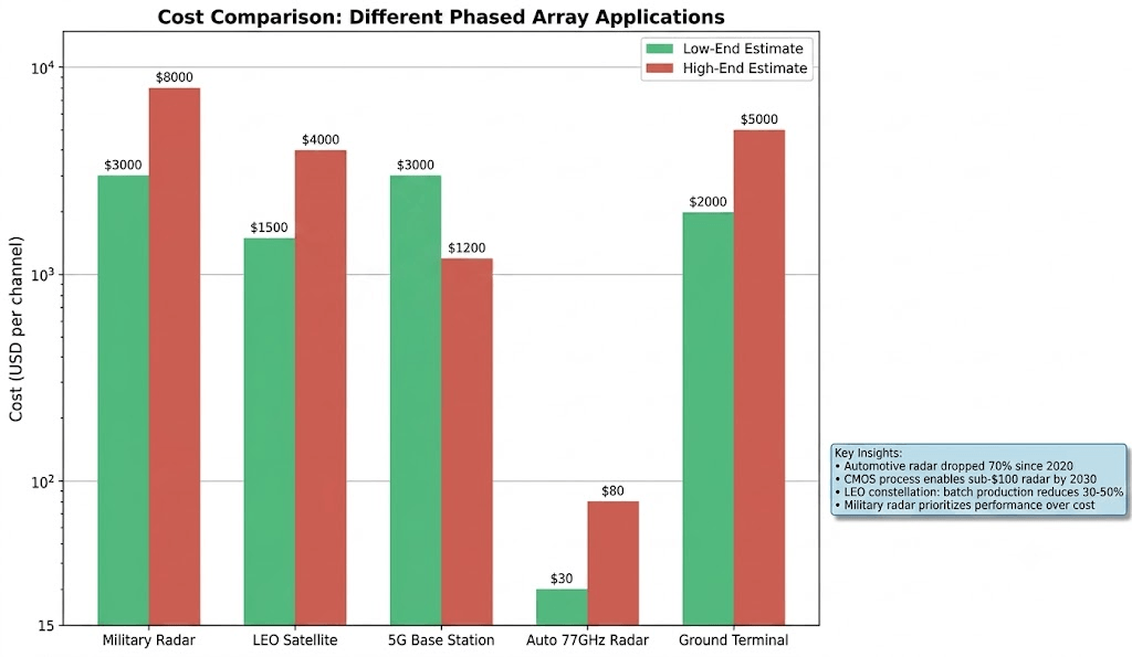
| Application Scenario | Target Cost Baseline | Primary Cost Reduction Focus |
| Military & Defense Radar | $750 – $1,500 / Channel | High performance takes precedence. Focus is on GaN + Full Digital Beamforming (DBF). |
| 5G Base Stations | $45 – $150 / Channel | Cost-sensitive mass deployment. Focus is on Hybrid Beamforming (HBF) + Modular Sub-array Reuse. |
| Automotive 77GHz Radar | $20 – $45 / Chip | Extreme cost pressure. Dominated by highly integrated CMOS Silicon + Antenna-in-Package (AiP) + Localization. |
| LEO Satellite Constellations | $300 – $450 / Channel | Balance of performance and volume. Focus is on batch manufacturing scale, Silicon-based RFICs, and Sparse Array thinning. |
| Satellite Ground Terminals | Hundreds of Dollars (Total) | Consumer-facing or commercial VSAT. Moving toward Liquid Crystal Phased Arrays to slash traditional costs by up to 90% |
Market Trend Note: Automotive mmWave radar presents the clearest cost-reduction curve in the RF industry. A standard sensor that cost around $45 (300 RMB) in 2020 dropped to roughly $22 (150 RMB) by 2024, and economies of scale are projected to push baseline chip-level solutions well below $30 in the coming years.
4. Next-Gen Technologies Changing the RF Cost Paradigm
Looking beyond current design tweaks, several emerging technologies are poised to completely disrupt the economics of phased array manufacturing
4.1 Silicon-Based Terahertz (THz) Integration
As CMOS technology advances into the millimeter-wave and terahertz frequencies, we can achieve massive economies of scale. In the future, fully integrated Silicon-based RFICs could drop T/R channel costs to under $10/channel, compared to the current $100–$500/channel standard for discrete high-frequency components. This represents a monumental order-of-magnitude shift.
4.2 Liquid Crystal Phased Arrays (LCPA)
LCPA is an exciting alternative to traditional active semiconductor arrays. By utilizing the voltage-controlled dielectric properties of liquid crystals (similar to display panel technology) to shift phases, commercial products (such as those from Huameitai Technology) have demonstrated a 90% reduction in manufacturing costs and drop power consumption to under 25% of active arrays, making them highly disruptive for satellite broadband terminals.
4.3 Glass-Substrate Holographic Digital Phased Arrays
Recent breakthroughs in glass-substrate holographic beamforming are attracting significant industry attention. By leveraging existing high-volume LCD/OLED display panel production lines, manufacturers can print antenna structures directly onto glass substrates. This technology achieves complex beam steering at a fraction of the cost—potentially one-tenth of traditional active phased arrays.
Final Thoughts: Choosing Your Cost-Reduction Matrix
Controlling the cost of a millimeter-wave phased array is a comprehensive systems engineering challenge. There is no single “silver bullet”. The most effective framework requires a phased combination of strategies:
Short-Term Wins: Prioritize chip localization, optimize hybrid PCB layer stack-ups, and simplify array architecture via thinning techniques.
Medium-Term Optimization: Implement Hybrid Beamforming architectures, enforce modular sub-array reuse, and transition to Automated Test Equipment (ATE).
Long-Term Innovation: Monitor and design for Silicon-based high-density integration, alternative substrates (Liquid Crystal/Glass), and Reconfigurable Intelligent Surfaces (RIS).
By carefully balancing your specific application constraints against your performance targets, you can deliver a design that satisfies both your engineering requirements and your finance department’s bottom line.
If you have more cost-reduction insights or unique challenges in your current design, feel free to reach out and connect. After all, for us engineers, sharing experiences and driving collective progress is how we push the industry forward.
Disclaimer: Hardware cost estimates and pricing structures provided in this article are based on aggregate market research and historical public industry data, intended for architectural reference and engineering estimation purposes only.