
In the world of millimeter-wave and terahertz technology, every decibel counts. You might have the most advanced RF source, but without a perfectly optimized waveguide, your signal could be dissipating as heat before it ever reaches its destination. From microscopic surface textures to the precision of a flange connection, even the smallest imperfection can lead to significant power loss.
In this guide, we dive deep into the physics of waveguide attenuation—exploring how factors like skin effect, surface roughness, and mechanical alignment impact your system’s performance—and more importantly, how you can minimize these losses to ensure maximum transmission efficiency.
Waveguide Insertion Loss Factors: Impact of Surface Roughness, Skin Depth, and Frequency
In high-frequency engineering, minimizing signal attenuation is critical for maintaining system efficiency. Whether you are working in telecommunications or industrial microwave applications, understanding the physical and electrical factors that cause waveguide loss is the first step toward superior design.
Below, we break down the primary sources of loss and provide actionable data to help you optimize your systems.
- Conductor Loss and the Skin Effect
The most prevalent form of attenuation is conductor loss, caused by the electrical resistance of the metal walls. As frequency increases, the skin effect forces current to flow only through a very thin surface layer, increasing effective resistance.
Material Selection: Copper is the standard due to its high conductivity (5.96×10⁷S/m), but lighter materials like aluminum are used despite higher losses.
Plating: Coating copper with silver can reduce losses by up to 20%.
Temperature Impact: Conductivity drops as temperature rises. A jump from 20°C to 50°C can increase conductor loss by 12%.
- The Critical Role of Surface Roughness
Surface finish is not just an aesthetic choice; it is a technical necessity. When surface roughness exceeds the skin depth of the signal, the current must travel a “longer” path over the microscopic peaks and valleys, leading to higher energy dissipation.
| Frequency (GHz) | Skin Effect (µm) | Roughness (µm) | Estimated Loss (dB/m) |
| 5 GHz | 0.93 | 0.5 | 0.02 |
| 5 GHz | 0.93 | 1.5 | 0.04 |
| 10 GHz | 0.66 | 0.5 | 0.03 |
| 10 GHz | 0.66 | 1 | 0.06 |
Pro Tip: For high-frequency systems (above 10 GHz), regular maintenance is required to prevent corrosion or deposits from increasing surface roughness over time.
- Dielectric and Impedance Losses
If your waveguide contains insulating materials (like PTFE or quartz supports), dielectric loss occurs as these materials absorb energy from the electromagnetic field. This is determined by the material’s loss tangent (tanδ) and its position within the guide.
Furthermore, Impedance Mismatch occurs when the waveguide’s characteristic impedance does not align with connected components like antennas or converters. This causes power to reflect back to the source, creating standing waves and potential “hot spots”.
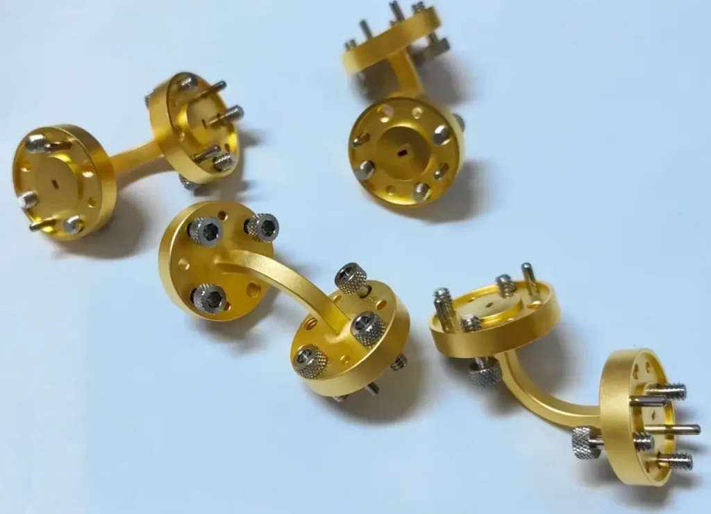
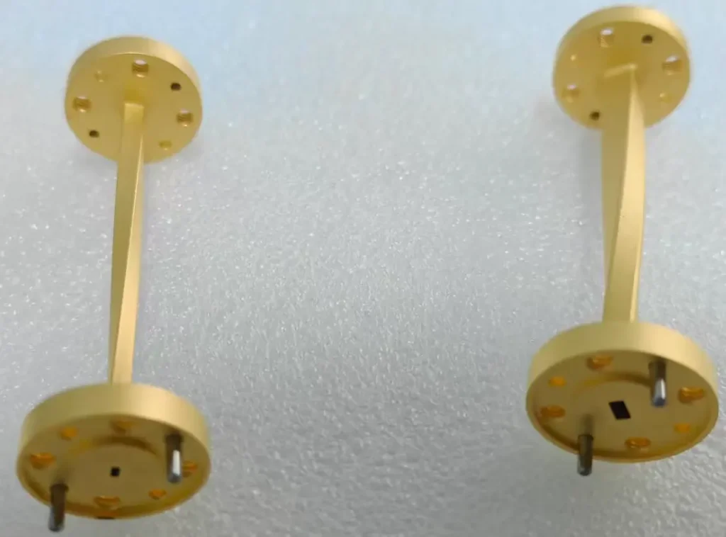
- Mechanical Geometry: Bends, Leaks, and Connections
The physical assembly of a waveguide system introduces several “mechanical” losses:
Bends: Changes in direction cause energy scattering. A standard 90° bend with a radius of 2ɑ (twice the waveguide width) typically loses 0.02 dB at 5 GHz.
Leaks: Energy can escape through gaps in flanges or poor welds. A tiny 0.1 mm gap in a flange can increase loss from 0.01 dB to 0.1 dB per joint.
Misalignment: Precise mechanical alignment is vital. A 0.1mm offset at a connection can result in a 0.05 dB loss per point.
Summary of Loss Mitigation Strategies
To maximize the efficiency of your 1 kW or high-power systems, consider these standard benchmarks:
| Factor | Mitigation Strategy | Efficiency Gain Example |
| Bends | Increase radius to ≥3a | Reduces bend loss by ~50% |
| Flanges | Ensure precision alignment | Avoids 0.1 dB/joint leakage |
| Surface | Use silver plating or polishing | Can save up to 8W per 10m (500W system) |
| Frequency | Design for specific TE10 modes | Minimizes mode conversion losses |
Precision is the Enemy of Attenuation
Reducing waveguide loss isn’t just about choosing the right material; it’s about mastering the details. Whether it’s selecting silver plating to boost conductivity by 20% or maintaining a surface roughness well below the skin depth, technical excellence is found in the microns. As systems move into higher frequency bands like 10 GHz and beyond, the margin for error disappears.
At THZ Precision, we specialize in the high-precision machining required to meet these rigorous standards. By focusing on superior surface finishes and exact mechanical tolerances, we help engineers push the boundaries of what’s possible in microwave and terahertz communication.