
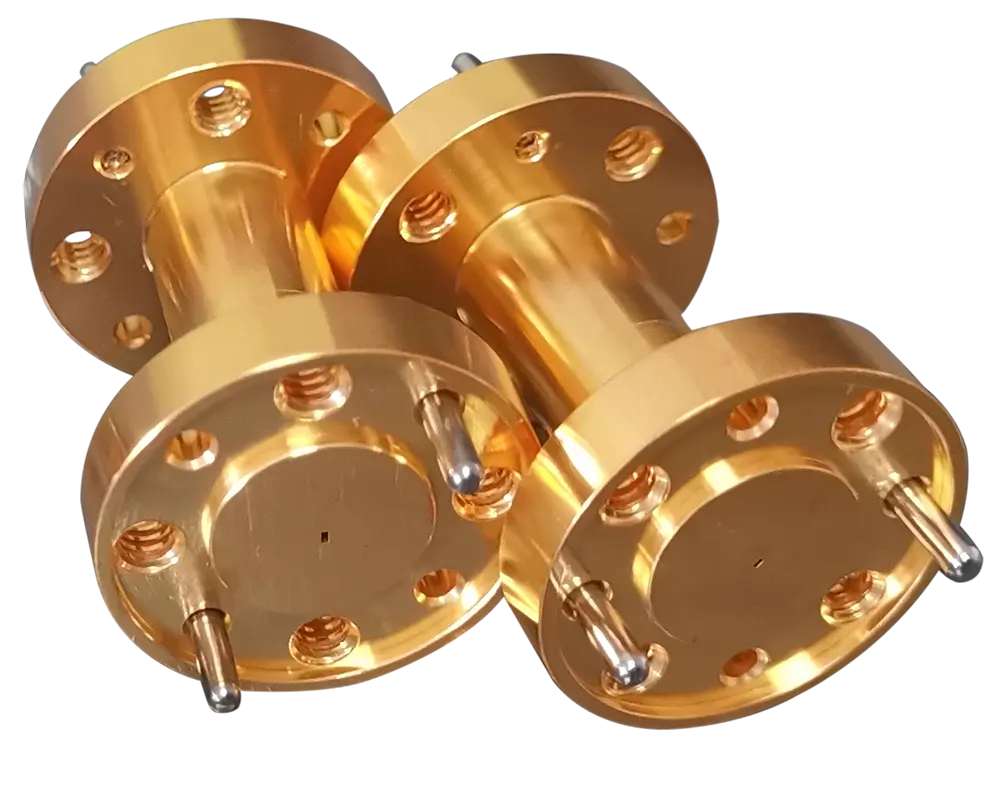
WR2.2 waveguides belong to the sub-millimeter and early THz regime, where electromagnetic behavior is highly sensitive to:
Micron-level dimensional accuracy
Surface roughness
Plating thickness
Flange alignment
Mode purity
Fabrication repeatability
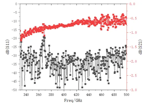
The test results demonstrate excellent electrical performance that validates both the mechanical precision and the manufacturing repeatability of the waveguide.
- S21 (Insertion Loss) Analysis — Red Curve
Measured range: ~ −0.4 dB to −1.2 dB
In the 330–500 GHz band, this insertion-loss level is exceptionally low for a 1-inch WR2.2 straight waveguide.
The S21 curve shows:
A smooth frequency response
No sudden resonant peaks
No evidence of higher-order mode excitation
Minimal mismatch-induced ripple
This indicates:
Excellent internal surface finish
High conductivity of the plating
Correct waveguide cross-sectional geometry
Very low propagation loss
Engineering conclusion:
The S21 performance is fully consistent with a high-quality, low-loss WR2.2 straight waveguide.
- S11 (Return Loss) Analysis — Black Curve
Measured range: −20 dB to −40 dB
A return loss between −20 and −40 dB at WR2.2 frequencies is considered high-grade performance.
The S11 data shows:
Strong impedance matching
Minimal flange mismatch
No internal cavity discontinuities
No machining-induced mode conversion
The small oscillations in S11 are normal and primarily caused by:
VNA extender noise floor
Mismatch in the test setup
IFBW / averaging settings
330–500 GHz system drift inherent to sub-mm-wave measurement
None of these fluctuations indicate a structural issue in the waveguide.
Engineering conclusion:
S11 performance confirms excellent impedance continuity and dimensional accuracy.
- Combined Performance Interpretation
When S21 and S11 are viewed together, the waveguide demonstrates:
Low insertion loss (<1.2 dB)
High return loss (−20 to −40 dB)
Smooth, stable frequency response
Uniform internal plating and low conductor loss
Precise rectangular cross-section with minimal deviation
Excellent flange mating and alignment repeatability
These characteristics are difficult to achieve at WR2.2 due to the ultra-small waveguide aperture (~0.56 × 0.28 mm).
- What These Results Mean for High-Frequency Applications
This WR2.2 1-inch waveguide meets the requirements for:
THz imaging systems
Sub-mm-wave spectroscopy
High-frequency communication modules
Vector network analyzer (VNA) calibration
Low-loss transmission in laboratory setups
Mode-purity-sensitive applications
The combination of low insertion loss and strong return loss ensures minimal measurement error and reliable system performance.
- Why This Performance Matters (SEO-Friendly Engineering Insight)
At 330–500 GHz, waveguides are extremely sensitive to:
Machining tolerances
Surface roughness
Plating thickness consistency
Waveguide straightness
Flange-to-flange alignment
Internal edge sharpness
This test validates that our WR2.2 manufacturing achieves:
- Sub-micron precision machining
- Low-roughness internal walls suitable for THz frequencies
- Uniform high-conductivity plating
- High repeatability for volume production
Such performance is essential for mmWave components, THz waveguide assemblies, and ultra-high frequency RF systems.