
Waveguides: High-Performance Transmission Lines for Microwave and THz Applications
Waveguides are a specialized form of transmission lines engineered for microwave applications. While conventional waveguides are constructed from metallic tubes—typically copper or brass, often silver-plated or gold-plated for enhanced conductivity—emerging technologies now utilize ultra-lightweight carbon fiber composites with electroplated copper.
Waveguides can feature rectangular, circular, or elliptical cross-sections. As transmission frequencies exceed 1 GHz, coaxial cables exhibit significant drawbacks in high-power scenarios, such as high attenuation and low flashover resistance. Attenuation losses, driven by line capacitance, inductance, and the skin effect, escalate with frequency. Above 36 GHz, coaxial cables become highly impractical due to extreme signal loss. Furthermore, the flashover and arc resistance in coaxial lines are severely limited by the narrow spacing between the inner and outer conductors.
While these limitations may be tolerable for low-power signals, they lead to unacceptable losses in high-performance and high-power ranges. Compared to coaxial lines, waveguides offer substantial advantages in terms of transmission loss. The electric and magnetic fields used for energy transmission are zero at the metallic surfaces, effectively confining the fields within the hollow space of the waveguide walls. Additionally, the electromagnetic fields are entirely contained and shielded. With virtually no radiation loss from inside-out or outside-in, waveguides provide exceptional interference immunity (EMI shielding).
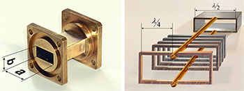
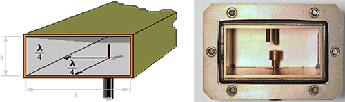
From Transmission Lines to Waveguides: The Physics of Resonant Stubs and Cut-off FrequenciesConventional two-wire transmission lines require support from insulators at regular intervals. To function efficiently, these insulators must exhibit extremely high impedance to ground at the connection point. At high frequencies, a superior alternative to physical insulators is the resonant stub —a matched, quarter-wavelength λ/4 short-circuited transmission line section. Through precise matching, this stub transforms the short circuit into an exceptionally high impedance at the junction with the main line.As more resonant stubs are added, each section eventually contacts the next, forming the walls of a rectangular waveguide. In this structure, the original two-wire line becomes part of the waveguide wall, with a total width defined by λ/2.It is important to note that a resonant stub acts as an insulator only at a specific frequency, which inherently limits the bandwidth and efficiency of energy transmission. Signals can only propagate within a waveguide above a specific cut-off frequency, which is determined by the waveguide’s broad dimension (“a”). Propagation occurs only when the wavelength is shorter than the cut-off wavelength λcutoff. In practice, a waveguide must be approximately 30% wider than this half-wavelength threshold for efficient operation.Waveguide specifications and descriptions comply with international standards such as IEC 153 and DIN 47302. For standard rectangular waveguides, the narrow wall (“b”) is half the size of the broad wall (“a”). For example, a waveguide section made from extruded brass tubing designated as WR42 follows this convention. The “WR” prefix stands for “Waveguide Rectangular,” and the numerical value represents the internal width in hundredths of an inch. Therefore, dimension “a” is exactly 0.42 inches (10.67 mm), and dimension “b” is 0.21 inches (5.34 mm). The lower cut-off frequency for WR42 is 14.051 GHz, with low-loss transmission typically beginning at 30% above this frequency.
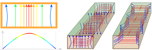
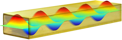
Field Distribution and Attenuation in Waveguides: The $TE_{10}$ Dominant ModeWhen electromagnetic energy is coupled into a waveguide, an electric field (E-field) is established at the center of the broad wall (“a”). This electric field is at its maximum intensity in the center of the waveguide and tapers off toward the narrow walls (“b”), forming a sinusoidal distribution across the cross-section.This oscillating electric field, in turn, generates a magnetic field (H-field). However, a critical boundary condition is that magnetic field lines cannot exist perpendicularly at the surface of a perfect metallic conductor. The electric field varies periodically over time and space, exhibiting maximum and minimum values at half-wavelength intervals along the longitudinal axis of the waveguide.The high-frequency energy fed into the waveguide supports Transverse Electromagnetic (TEM) modes in certain contexts, but within the physical constraints of a rectangular metallic waveguide, the fields are primarily Transverse Electric (TE) or Transverse Magnetic (TM). Specifically, for the dominant TE10 mode, the electric field lines are established between the two broad walls, while the magnetic field loops are situated between the two narrow walls.
Waveguide Attenuation and Frequency: Impact of Wall Current LossesThe attenuation within a waveguide is intrinsically linked to its operating frequency. Near the cut-off frequency, a waveguide exhibits relatively high attenuation. As the frequency increases, the attenuation decreases until it reaches a minimum. This optimal operating range remains relatively stable over a certain bandwidth before the attenuation begins to rise again at higher frequencies.The decisive factor for maintaining low-loss conductivity in a rectangular waveguide is its physical dimension
—
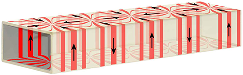
specifically the broad wall (“a”) relative to the operating frequency. If the wavelength is too large, the peak voltage lacks sufficient space to propagate efficiently. Consequently, higher frequencies necessitate smaller waveguide dimensions, and vice versa.[Image showing the attenuation-frequency curve for a typical rectangular waveguide]Wall Current Distribution and Loss MechanismAttenuation is primarily driven by losses from wall currents. Figure 4 illustrates the surface current distribution for the TE10 mode. The longitudinal wall currents flow along the center of the top and bottom walls in the direction of propagation. Additionally, transverse currents flow toward the edges (narrow walls). The attenuation constant for a given mode can be accurately estimated by calculating the surface integral of the wall current density.
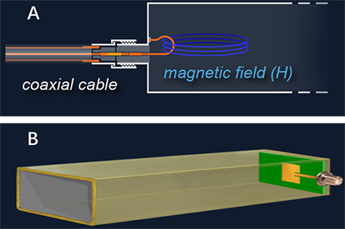
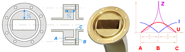
Waveguide Wall Conductivity and Excitation Methods: Probe CouplingIn a waveguide, wall currents flow exclusively on the inner surfaces at the speed of light. To minimize resistive losses, waveguide walls are typically constructed from polished brass. It is imperative that the inner surfaces maintain exceptionally high conductivity. For enhanced performance, these surfaces are often silver-plated or — specifically for frequencies above 40 GHz — gold-plated to prevent oxidation and ensure long-term stability.Waveguide Input/Output Methods: The Quarter-Wave ProbeA common method to excite or extract microwave energy is through a small probe inserted into the waveguide, which functions as a quarter-wavelength λ/4 antenna. As current flows through the probe, an electric field (E-field) is established, as illustrated in Figure 5. When the probe is positioned at the point of maximum efficiency, the E-field lines radiate with optimal intensity.The most effective location for the probe is at the center of the broad wall (“a”), oriented parallel to the narrow wall (“b”). To achieve maximum energy transfer (coupling), the probe should be positioned exactly one-quarter wavelength λ/4 from the short-circuited end of the waveguide. At this specific location, the E-field of the dominant mode is at its peak. In this resonant state, the probe behaves similarly to a monopole antenna, where the H-plane is parallel to wall “a” and the E-plane is perpendicular to wall “a”.
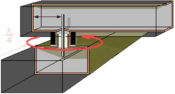
Advanced Waveguide Excitation: Impedance Matching for Probes and Loop CouplingIn rectangular waveguide probe coupling, the electric field (E-field) is generated first, which subsequently establishes the magnetic field (H-field). However, a practical challenge arises in achieving optimal impedance matching between the probe and the feeding cable. Ideally, the probe length should be slightly longer than λ/4 to ensure a robust transition; however, this often conflicts with the narrow wall (“b”) dimension, which is typically only slightly larger than a quarter-wavelength.This physical constraint introduces unwanted capacitive reactance. To counteract this effect and achieve a perfectly matched resonant state, a tuning screw is often implemented on the opposite wall (as shown in Figure 5, right). This configuration creates an opposing inductive or capacitive effect, allowing for a tunable resonant frequency and superior return loss performance.Magnetic Field Excitation: Loop Coupling MethodAn alternative method for injecting energy into a waveguide is to establish an H-field directly via loop coupling. This is achieved by inserting a small conductive loop carrying high current into the waveguide, as illustrated in Figure 6. The magnetic field forms around the loop and expands into the waveguide interior. If the frequency of the current within the loop falls within the waveguide bandwidth, energy is efficiently transferred into the system.
Optimizing Waveguide Coupling: Loop Feeds and Microstrip Transitions
To achieve maximum coupling efficiency, a loop must be positioned at one of the locations where the magnetic field intensity is at its peak. In loop coupling within a rectangular waveguide, the magnetic field (H-field) is generated first, which subsequently establishes the electric field (E-field).
Modern engineering often utilizes patch antennas or microstrip feeds for energy injection. In this configuration, a conventional microstrip patch antenna is integrated at the waveguide aperture and fed via a coaxial line. Theoretically, the intensity of the energy transmitted into the waveguide depends on the operating mode and radiation efficiency of the microstrip antenna. To minimize energy coupling loss, the microstrip antenna should be positioned as centrally as possible. However, it is important to note that the presence of dielectric substrates in microstrip designs introduces inherent material losses, particularly at higher frequencies.
Electromagnetic Propagation Modes
A waveguide can support the propagation of multiple electromagnetic modes. The physical dimensions of the waveguide dictate the cut-off frequency for each specific mode. If the frequency of the applied signal exceeds the cut-off frequency of a given mode, electromagnetic energy can be transmitted with minimal attenuation. Conversely, if the signal frequency falls below the cut-off threshold, the energy will be attenuated to a negligible value over a very short distance (evanescent waves).
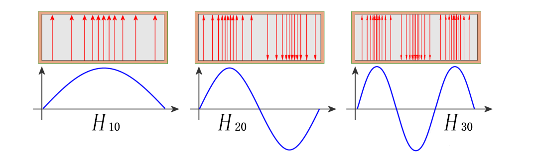
dominant mode in a specific waveguide is the mode with the lowest cut-off frequency. For rectangular waveguides, this is the TE10 mode. The designation TE (Transverse Electric) signifies that all electric field components are transverse to the direction of propagation, with no longitudinal electric field present. Conversely, the magnetic field does possess a longitudinal component; therefore, TE modes are also referred to as H-modes.As shown in Figure 7, the subscripts m and n define the field distribution: m represents the number of half-wave patterns across the waveguide width (“a”), while n represents the number across the height (“b”).Ensuring Single-Mode PropagationTo maintain signal integrity, waveguide dimensions must be carefully selected so that only the dominant mode energy can propagate at the given operating frequency. If a rectangular waveguide is too wide for a specific frequency, the TE20 mode may be excited, leading to significant interference and phase distortion. In standard rectangular waveguides with low aspect ratios, TE20 is the next higher-order mode and is harmonically related to the TE10 cut-off frequency. This critical relationship—along with attenuation and propagation constraints — defines the normal operating frequency range (typically 1.25×fc to 1.9×fc of a rectangular waveguide
Double-Ridged Waveguides and Connection Technologies: From Choke Joints to Rotary Unions
Another widely utilized architecture is the double-ridged rectangular waveguide. The integration of internal ridges significantly extends the operating bandwidth of the waveguide, albeit at the cost of higher attenuation and reduced power-handling capacity compared to standard rectangular types.
Waveguide Connection Methods
Since complex waveguide systems cannot be manufactured as a single monolithic structure, they must be constructed in discrete segments and joined at interfaces. There are three fundamental types of waveguide connections:
Permanent Joints: These are factory-welded or brazed connections designed for maintenance-free operation and maximum structural integrity.
Semi-Permanent Joints (Choke Joints): When sections must be disassembled for maintenance or repair, choke joints (choke flanges) are the industry standard. A choke joint ensures excellent electromagnetic continuity between waveguide sections with minimal power loss and leakage.
Rotary Joints: Whenever a stationary waveguide system must connect to a rotating antenna, a rotary joint is required. Circular waveguides are commonly employed within these joints to facilitate rotation. The rotating interface typically incorporates a choke joint to maintain a stable electrical connection with the stationary section.
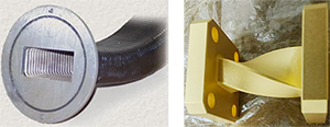
Principles of Waveguide Choke Joints and Coaxial-to-Waveguide Rotary JointsThe cross-sectional view illustrates the sophisticated design of a waveguide choke joint. A pressure washer (O-ring) situated between the two metallic surfaces creates an airtight seal, which is essential for pressurized systems.In this architecture, the distance from the waveguide broad wall (“a”) to the circular ditch is precisely 1/4λ. The depth of this ditch is also 1/4λ . Since the end of the ditch is a physical short-circuit, it creates an infinite (high) impedance at the 1/4λ point. According to transmission line theory, this high impedance is transformed into a zero (low) impedance — or an effective short-circuit — at the 1/2λ point (the flange interface).This resonant effect establishes excellent electrical continuity between the two sections, allowing energy to propagate with minimal reflection or insertion loss. Consequently, a virtual conductive connection is achieved without requiring a direct mechanical DC contact between the flange faces, providing sufficient space to install hermetic seals for high-pressure applications.Rotary Joints and Probe CouplingRotary joints are indispensable for transmitting high-frequency energy from a stationary system to a rotating component, such as a radar antenna. Internally, these joints often utilize circular waveguides or short coaxial sections positioned at the center of rotation. As shown in Figure 10, probes are employed to couple RF energy between the waveguide and the coaxial section. It should be noted, however, that due to the inherent resonance of the probe structure, the operating bandwidth of this type of transition is relatively narrow compared to other coupling methods.
Mode Control in Rotary Joints and Principles of Waveguide Bending and TwistingCircular waveguide sections are frequently integrated into rotary joints. These sections are precision-engineered to propagate electromagnetic waves in the TE10 mode. To suppress unwanted higher-order modes, resonant vanes (slats) with a length of 3/4λ are implemented to create a high-impedance barrier against parasitic interference.Waveguide Bends and Twists: Maintaining Signal Integrity To ensure maximum energy transfer with minimal reflection, the dimensions, geometry, and dielectric properties of a waveguide must remain constant throughout its entire length. Any abrupt structural discontinuity can lead to significant reflections and a reduction in overall system efficiency. When a change in direction or orientation is required, waveguide bends, twists, and joints must be designed to meet specific electromagnetic criteria.Waveguides can be bent in several ways without inducing reflections. One standard method is the gradual bend, as illustrated in the accompanying diagram. This configuration is specifically known as an E-plane bend because it distorts the electric field orientation. To effectively prevent signal reflections, the radius of an E-plane bend must be greater than two wavelengths (>2λ).
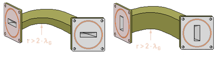
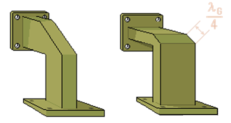
H-plane Bends and Mitered Bends: Advanced Reflection Cancellation TechniquesAn H-plane bend is so designated because the curvature occurs in the plane of the magnetic field (H-field). Similar to E-plane bends, the radius of a gradual H-plane bend must exceed two wavelengths (>2λ) to effectively suppress internal reflections.However, in systems where space is limited, sharp bends (mitered bends) can be implemented if specific electromagnetic requirements are met. One such method involves using two 45-degree mitered bends spaced exactly one-quarter wavelength (1/4λ) apart, as illustrated. In this configuration, the reflections generated at the first 45-degree junction are precisely canceled out by those at the second junction through destructive interference. This phase-cancellation effect allows the electromagnetic field to propagate as if no reflection had occurred, maintaining high system efficiency in a compact footprint.
Waveguide Twists and Flexible Waveguides: Polarization Control and System VersatilityOccasionally, the electromagnetic field must be rotated to align its polarization with the phase of the load. This is achieved by twisting the waveguide, as illustrated. To maintain signal integrity and prevent reflections, the twist must be progressive and extend over a length greater than two wavelengths (>2λ).Flexible Waveguides: Applications and LimitationsFlexible waveguides provide the adaptability required for specialized applications where static routing is impractical. These are typically constructed from a specially wound ribbon of conductive material—most commonly brass— with a chrome-plated inner surface to enhance durability.However, it is important to note that flexible waveguides exhibit significantly higher insertion loss compared to rigid versions. Because the inner surfaces are not perfectly smooth due to the interlocking ribbon structure, they introduce increased attenuation and reduced power-handling capacity.
Waveguide Impedance Matching: Inductive Irises and Equivalent Circuits
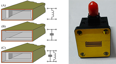
Waveguide impedance matching is a critical requirement for minimizing reflections caused by mismatches between the waveguide and its connected load. Inductive impedance matching and its corresponding equivalent circuit are illustrated in Figure (A). In this configuration, the integrated metallic partitions—commonly known as inductive irises (diaphragms)—generate a shunt (parallel) inductance across the waveguide.
The magnitude of this inductive reactance is directly proportional to the size of the opening (aperture), where the edges of the metallic iris are oriented perpendicular to the magnetic plane (H-plane).
Capacitive Irises, Resonant Windows, and Waveguide T-Junctions
Capacitive impedance matching (as illustrated in View B) functions similarly to inductive matching. The capacitive reactance generated is proportional to the aperture size, but in this configuration, the metallic edges are oriented perpendicular to the electric plane (E-plane).
When the metallic structures span both the magnetic and electric planes, as shown in View (C), they form an equivalent parallel LC circuit across the waveguide. This is known as a resonant window. At the resonant frequency, the metallic iris acts as a high shunt resistance. Above resonance, it exhibits capacitive reactance, while below resonance, it behaves inductively. In addition to irises, conductive posts and tuning screws are also extensively used for precision impedance matching within waveguide systems.
Waveguide Transitions and Junctions
When a waveguide system requires the combination of two or more signals (or the splitting of a signal into multiple paths), various types of junctions are employed. The “T-Junction” is the most fundamental and widely used waveguide connector. T-junctions are categorized into two primary types: E-plane (Series) Tees and H-plane (Shunt) Tees.
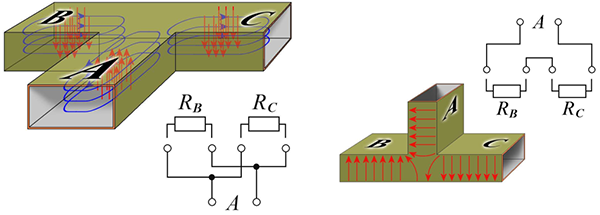
Waveguide T-Junctions and the Magic-T Hybrid JunctionAn H-plane T-junction is illustrated in Figure 15 (left). This designation is used because all three arms are situated within the magnetic field plane, allowing the H-field to be divided between the arms. When an electric field is fed into Arm A, the outputs obtained from Arms B and C are in-phase. Conversely, the junction can also function in reverse to combine signals.The right-hand image depicts an E-plane T-junction. This junction is characterized by metallic walls extending from the main waveguide in the same direction as the electric field. Due to the series nature of this connection, the outputs between the two arms exhibit a 180°
phase difference (out-of-phase).The Magic-T Hybrid JunctionA simplified version of the Magic-T hybrid junction is shown in Figure 16. The Magic-T can be described as a dual-electromagnetic plane T-junction, effectively combining the characteristics of both H-plane and E-plane types.In this architecture, Arms B and C are referred to as the collinear arms or side arms. Arm D is designated as the “Difference Port”, while Arm A is known as the “Sum Port” . Magic-T junctions are most commonly utilized as balanced mixers in microwave radar receivers or as critical components in high-precision measurement systems.
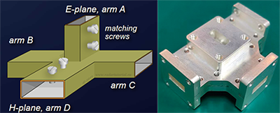
Port Isolation and Boundary Conditions in Magic-T Junctions
If a signal is fed into the E-plane arm (Arm A) of a Magic-T, it will divide into two equal components at the collinear arms (Arm B and Arm C) with a 180° phase difference (out-of-phase).
A critical functional characteristic is that the signal entering the E-arm will not propagate into the H-plane arm (Arm D). This occurs because a zero potential (null point) is established at the entrance of the H-plane arm. To satisfy the electromagnetic boundary conditions of the E-plane arm, the potential at the junction intersection with the H-arm must remain zero, ensuring high cross-port isolation.